Fast, local cryopreservation is a consistent bottleneck for autologous cell therapy developers, even in major cell and gene therapy hubs. For the peripheral blood mononuclear cells (PBMCs) that form the foundation of immunotherapies, vaccine development and autologous therapies, every hour between leukapheresis collection and cryopreservation can degrade cell viability and functional integrity.
OrganaBio’s new PBMC isolation facility in San Diego removes that bottleneck for one of the three major cell and gene therapy hubs in the world. The opening of the new PBMC processing and cryopreservation laboratory at Excellos Labs (which OrganaBio acquired in May) makes it possible to isolate and cryopreserve PBMCs within three to four hours of collection, rather than losing time and quality by shipping live material across the country.
“The quality you lock in at cryopreservation is the quality the developer gets back months later,” Justin Irizarry, CEO, OrganaBio, tells GEN. “Get the first few hours right and you have protected everything downstream. Having that processing happen locally is what makes the few-hour window realistic rather than aspirational.”
The San Diego lab reports an average PBMC viability of “around 99.1% and recovery above 2.9 million cells per milliliter, with consistency from batch to batch,” Irizarry says. He credits those statistics to rapid time to cryopreservation, validated standard operating procedures “including sponsor-specific protocols,” personnel trained in each of those procedures, and a single quality system for each of OrganaBio’s sites. That combination ensures consistency across batches and sites, so “a sample processed in San Diego is indistinguishable from one processed in Miami,” he emphasizes.
In contrast, one German study comparing cells cryopreserved within six hours or 20 hours of collection notes a higher percentage of apoptotic natural killer (NK) cells associated with the longer hold time. Specifically, after 20 hours, 41% of the cells were apoptotic versus 24% for those preserved within six hours of collection. Robustness also declined with the longer hold times.
Robust local sourcing for PBMCs is a strategic advantage for San Diego’s clinical-stage biotherapeutic developers. In addition to gaining higher-quality starting materials, they can expect to benefit from tighter manufacturing timelines and less supply chain risk. Local processing reduces the inherent risk associated with cold-chain and transportation variables, while enhancing redundancy provided by OrganaBio’s West Coast sites in San Diego, Irvine, and San Francisco Bay, and its East Coast headquarters in Miami.
OrganaBio expects continued growth, “including clinical trial services, manufacturing services, and product manufacturing,” Irizarry says. The company is onboarding new customers and programs and deepening relationships with existing customers. “We also will evaluate opportunities to expand into additional markets for clinical trial services, particularly where there is strong population growth, good ethnic and racial diversity, and a lack of professionalized PBMC isolation services in the market.”
IntroductionPediatric-psychosomatic inpatient therapy is an essential part of the German health care system for the treatment of mental disorders in children and adolescents. However, empirical research in this field remains scarce and limited to psychological parameters. This longitudinal naturalistic study aimed to evaluate the efficacy and sustainability of inpatient psychosomatic therapy in children and adolescents by examining both psychological outcomes and biological markers.MethodsA total of 58 patients were assessed at seven time points before, during, and after treatment. Hair cortisol concentration (HCC) was measured as a neuroendocrine parameter of long-term stress regulation. Psychometric data were collected using five validated questionnaires.ResultsFindings indicated significant improvements in perceived stress, depressive and anxiety symptoms, family functioning and internalizing symptoms in the course of inpatient treatment. Overall, these effects remained stable at three- and six-month follow-ups, with only transient increases in depressive symptoms and family problems. HCC showed a significant decrease from admission to discharge and remained stable across follow-ups.DiscussionThese results support the efficacy of inpatient pediatric psychosomatic interventions on both psychological outcomes and neuroendocrine stress regulation and highlight the value of integrating biological markers into psychotherapy research.
Huntington’s disease is a devastating brain disorder in which damage to nerve cells leads to progressively worsening cognitive and movement abilities. While the genetic mutation responsible for the condition is well known, the details of how the disease disrupts brain circuits have not been clearly understood. Now, researchers have identified and tracked neurons involved in Huntington’s disease progression and used optogenetics to selectively activate these neurons and improve the debilitating deficits of the condition.
“This work shows that correcting specific imbalances in brain circuits can restore function, even in a complex neurodegenerative condition, and highlights the potential of targeting defined cell types to promote recovery,” said Takaki Komiyama, PhD, professor in the UC San Diego Departments of Neurobiology (School of Biological Sciences) and Neurosciences (School of Medicine).
Huntington’s disease is caused by a trinucleotide repeat mutation in the Huntingtin (HTT) gene. While the mutation is well known, the neural networks connected with the disease progression have been more elusive.
This work aimed to map the neural circuits that expose the networks involved at the onset and spread of the disease’s debilitating symptoms. In transgenic mice carrying the same mutation as human patients, the researchers evaluated how different types of brain cells in the motor cortex are affected in Huntington’s disease. Advanced imaging techniques allowed the researchers to track the activity of these cortical neurons as the disorder progressed.
The researchers found that the disease disrupts the balance of activity across different cell types, including cortical inhibitory neurons.
“Cortical inhibitory cells have received little attention in Huntington’s disease, as for a long time they were considered to be spared from neurodegeneration,” said Irina Dudanova, PhD, previously based at the Max Planck Institute for Biological Intelligence, now at the University of Würzburg in Germany. “Surprisingly, we detected profound changes in their activity, with some cell types being overactive and some nearly silent.”
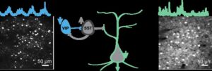
The activity of neuron types in the brain is imbalanced in mice with Huntington’s disease. The image depicts an example field-of-view from inhibitory (left) VIP (vasoactive intestinal peptide) neurons and excitatory (right) neurons recorded during behavior. Activity traces from a selected neuron for each type are shown above the images. [Sonja Blumenstock, Komiyama Lab, UC San Diego]
In particular, a class of inhibitory neurons known as vasoactive intestinal peptide (VIP) neurons, exhibited significantly reduced activity. VIP neuron activity is essential for normal learning, as these cells enable the brain to adapt and refine brain circuits during learning.
Reduced VIP neuron activity, the researchers reasoned, could be impairing the brain’s ability to function and learn properly. They sought to activate these cells to re-engage brain states that support learning. They tested this idea using optogenetics to stimulate VIP neurons.
“By activating the VIP inhibitory cell type, we gradually restored more normal activity patterns, and, very importantly, we also saw an improvement in the ability of the mouse to learn a motor task,” said Sonja Blumenstock, PhD, assistant project scientist at UC San Diego.
The results confirm VIP neurons as a key point of vulnerability in Huntington’s disease as well as a promising target for therapy. As to how this process works, the results suggest that modulating VIP neurons opens a “gate” that enables learning-related brain plasticity.
“This intervention restored more normal patterns of activity in the brain and improved movement in affected mice,” said Komiyama. “Importantly, the improvements persisted for days after stimulation ended, suggesting that the treatment triggered lasting beneficial changes in brain circuits rather than only temporary effects.”
The study provides important indications of where research could focus to normalize human brain function and facilitate brain recovery. Komiyama envisions a future scenario in which scientists could non-invasively activate the brain from outside the skull using novel approaches.
“Our study shows that despite the genetic defect, a precise intervention into the brain circuitry can lead to significant improvements in motor symptoms,” said Dudanova. “If we know which cells to target, we can retune the brain’s abnormal activity patterns. This gives hope for future therapies.”
The research also shows that corrections to specific brain circuit imbalances can restore function in a highly complex neurodegenerative condition, with similar potential in other disorders.
“We have come up with a way to allow the diseased brain to learn better,” said Komiyama. “The approach can improve behavior in diseased mice, and our hope is that a related approach will help people with impairment in their learning abilities.”
Norway-based Circio and Tcelltech, based in Germany, will collaborate using the double-stranded, non-integrating nanoSMAR vector platform for the development of next generation engineered T-cell therapies.
Engineered T-cell therapies such as CAR-T have transformed the treatment of certain cancers. However, ex vivo manufacturing remains complex, and the shift towards in vivo approaches currently relies on viral vectors that have significant safety concerns, according to Richard Harbottle, PhD, head of vector technology and manufacturing at Tcelltech. By integrating the technologies developed by Circio and Tcelltech, the parties aim to engineer T-cells with enhanced and sustained CAR/TCR expression, without the need for viral vectors, he adds.
“The combination of Tcelltech’s non-viral, episomal nanoSMAR DNA vector platform with Circio’s circVec expression technology holds great promise for the development of in vivo gene delivery systems that are non-disruptive to target cells, maintain high expression levels, and enable straightforward, cost-effective manufacturing,” says Harbottle. “Furthermore, the exceptionally large cargo capacity of nanoSMAR vectors—beyond what is achievable with viral approaches—enables the design of complex, and sophisticated constructs incorporating multiple payload genes and regulatory elements.”
Circio and Tcelltech will combine Circio’s circVec circular RNA expression technology with Tcelltech’s non-viral, high-cargo capacity nanoSMAR vector platform and evaluate the combination in engineered T cells through a staged research program. An initial proof-of-concept phase will compare how strongly and how durably the different technology combinations drive gene expression in primary human T cells, followed by a functional phase in which CD19-directed CAR T cells are generated and tested for their ability to kill tumor cells.
“In vivo T-cell therapy is one of the most exciting frontiers for our circVec technology and is a rapidly advancing approach that could make these therapies more scalable and accessible,” adds Victor Levitsky, PhD, CSO of Circio. “Tcelltech´s universal nanoSMAR platform is a promising and differentiated delivery technology for T-cells, which we expect will act synergistically with circVec-enhanced payload expression.
“This collaboration fits into Circio’s broad business development strategy of testing circVec across multiple modalities and delivery systems to identify the optimal technology combination and identify the most promising therapeutic avenues.”
Merck KGaA, Darmstadt, Germany, has agreed to acquire Bio-Techne for approximately $11.3 billion, the companies said today, in a deal designed to position the buyer as more of a leader across the life science value chain by expanding its presence in high-growth, next-generation life-sci markets with Bio-Techne’s tools, analytical technologies, and consumables.
The deal would add Bio-Techne’s multiomics offerings, analytical technologies, and integrated workflow solutions to German Merck’s platforms and services in research, bioprocessing and advanced therapeutics, with the aim of creating a combined company capable of helping customers from discovery and translational research through development, testing and commercial manufacturing.
Merck KGaA added that acquiring Bio-Techne would directly deliver on its mid- to long-term strategic agenda, which focuses on adding to its high-growth value drivers, integrated workflows, platformed capabilities—as well as scaling and sourcing innovation through merger-and-acquisition (M&A) deals like the Bio-Techne transaction.
Merck KGaA said it would also benefit from Bio-Techne’s position as a leading provider of materials, analytics, and process technologies to cell therapy developers. Bio-Techne expects to acquire the ownership in Wilson Wolf it does not own immediately following the end of calendar year 2027 under the terms of a two-part forward contract between the company and Wilson Wolf, a manufacturer of cell culture devices, including the G-Rex product line. Bio-Techne holds 19.9% of Wilson Wolf that it acquired in the fiscal year that ended June 30, 2023.
Merck KGaA employs more than 14,000 people in the U.S. across over 70 company and customer sites.
The $11.3 billion Bio-Techne acquisition is the new third largest biopharma merger-and-acquisition (M&A) deal announced so far this year, behind the €10.7 billion ($12.268 billion) cash buyout offer for Italian-based Recordati being pursued by CVC Capital Partners and Groupe Bruxelles Lambert, which aim to take the company private; and Sun Pharmaceutical Industries’ planned $11.75 billion purchase of Organon, the women’s health drug developer spun out of Merck & Co., in a deal expected to close in early 2027.
“Bio-Techne is an outstanding fit that directly supports our strategic direction focused on delivering cutting-edge products and solutions across the entire industry value chain—from lab customers to those manufacturing in the biotech and pharmaceutical industries,” Kai Beckmann, chairman of the executive board and group CEO of Merck KGaA, Darmstadt, Germany, said in a statement.
“By combining Bio-Techne’s scientific depth, innovation engine and differentiated portfolio with the global scale, manufacturing excellence and customer reach of Merck KGaA, Darmstadt, Germany, we are in a strong position to address some of the most important opportunities in life sciences and support our customers in accelerating the next generation of scientific discovery and therapeutic innovation. This positions us to deliver compelling strategic and financial benefits for shareholders, customers and employees,” Beckmann added.
Those benefits, according to German Merck, include immediate accretion to the company’s earnings before interest, taxes, depreciation, and amortization (EBITDA) pre margin for both the Group as a while and its Life Science business segment upon closing of the acquisition deal.
The Life Sciences segment finished last year with €8.98 billion ($10.36 billion) in revenue. Merck KGaA does not break down its businesses further than its three segments, which also include healthcare (drug development, focused on oncology, neurology and immunology, and “global health” treatments such as for malaria) and electronics (high-tech materials).
The deal is expected to close by late 2026 or early 2027, subject to satisfying customary closing conditions that include obtaining regulatory approvals and approval by Bio-Techne shareholders.
Bio-Techne’s board of directors and the corporate bodies overseeing Merck KGaA, Darmstadt, Germany, have already approved the transaction, which will also add to earnings per share (EPS) by year three after closing, German Merck said.
€140M in “synergies”
Merck KGaA said it will carry out cost-cutting “synergies” of approximately €140 million (about $159.3 million) that are expected to be fully realized by the third year after closing.
The planned acquisition will be funded through a combination of existing cash on hand and proceeds from new debt, Merck KGaA said, adding that it will preserve its “strong” investment-grade credit rating.
For Minneapolis-based Bio-Techne, the acquisition is expected to increase its geographic and omnichannel access for its customers through integration of its offerings with those of Merck KGaA through a synergistic platform.
Bio-Techne has more than 3,000 employees, with approximately 2,300 employees based in the U.S. The company operates 34 global locations and 15 manufacturing facilities across the U.S., Canada, the U.K., Switzerland and China, and generated net sales of more than $1.2 billion in the fiscal year that ended June 30, 2025.
A leader in recombinant proteins with a half-century of heritage in next-generation R&D and new modalities, Bio-Techne said it would bring to German Merck a globally recognized portfolio of cytokines, growth factors, antibodies, and immunoassay kits. Bio-Techne is expected to strengthen the analytical and bioprocess solutions of Merck KGaA by adding to its offerings ProteinSimple, a leader in automated protein detection and analysis instruments. Bio-Techne added that its RNAscope and related in situ hybridization technologies would strengthen the capabilities of Merck KGaA, in spatial biology and diagnostics.
“For 50 years, Bio-Techne has enabled scientific breakthroughs across proteomics, spatial biology, and novel therapeutics,” stated Kim Kelderman, president and CEO of Bio-Techne. “This transaction is a testament to the remarkable company our team has built and to the enduring value we create for our customers and stakeholders.”
Muted enthusiasm
Bio-Techne investors appeared to share only muted enthusiasm for the deal, as the company’s shares traded on Nasdaq rose just 19.8% to $70.53 as of 12:48 pm ET, from Wednesday’s close of $58.88 per share. Merck KGaA shares traded on XETRA rose 4.93% to €147.00 ($167.25).
Puneet Souda, senior managing director, life science tools and diagnostics, and a senior research analyst with Leerink Partners, offered a possible explanation in a research note today: “The acquisition appears to be only a 24% premium to yesterday’s close and 26x the Street’s forecast for FY27 [enterprise value]/EBITDA compared to 16x for its LST [life science technologies] peer group.”
“We see the acquisition multiple undervaluing what is a highly accretive asset in our view,” Souda wrote. “Historically, TECH [Bio-Techne’s stock ticker] traded at much higher multiples given their highly accretive consumables profile (80%+ consumables) of consistent 70%+ gross margins and operating margin potential.”
One rival company in particular may benefit from the deal, Souda said: “The announcement is likely to be viewed positive for peer LST companies today, especially RVTY [Revvity] in our view.”
At $73 per share cash, the deal price represents a 36% premium to Bio-Techne’s one-month volume weighted average trading price.
“As part of Merck KGaA, Darmstadt, Germany, we will have greater scale and expanded capabilities to accelerate innovation and deepen our impact. Together, we will empower our customers to tackle the most important challenges in science and healthcare, helping to improve outcomes worldwide,” Kelderman added.
WASHINGTON — The Supreme Court sided with the maker of Roundup weedkiller Thursday in a ruling expected to block thousands of lawsuits alleging it failed to warn people the product could cause cancer.
The case came before the justices after a tidal wave of litigation that included some multibillion-dollar verdicts against the global agrochemical manufacturer Bayer, a Germany-based company that acquired Roundup when it bought its original producer Monsanto in 2018.
Research led by the Technical University of Munich shows that data from some individuals used to train medical artificial intelligence (AI) models could be at much higher risk of exposure due to cyberattack than others.
Writing in Nature, the researchers explain that underrepresented groups, such as people with a rare disease or a minority ethnicity, are at particularly high risk of having their data exposed.
A type of cyberattack called a “membership inference attack” can be used to uncover sensitive information about individuals or learn about the training data behind an AI system, without seeing the original database. In the wrong hands, this kind of information can be used for discrimination, blackmail, or even to assess who might be vulnerable to exploitative marketing.
“The extent to which this constitutes a privacy violation is nuanced and depends on factors such as the underlying training population and the deployment context of the model. Although inferring membership for a model trained on a general population may be benign, doing so for a model trained on a narrow, disease- or center-specific cohort acts as a direct proxy for sensitive medical information,” explained lead author Moritz Knolle, a doctoral researcher at the Technical University of Munich, and colleagues.
In this study, the team studied seven large, real‑world clinical datasets including medical images, electrocardiograms, and electronic health records. They trained around 200 versions of an AI model for each dataset, then quantified, for every single record and patient, how accurately an attack would be at guessing if a patient was part of the training set.
They showed that membership inference attacks can be almost perfectly successful for some individual patients, such as those with an unusual disease or presentation, even though the average attack performance across the whole training set looked close to random guessing.
As the AI model capacity increased, the number of highly vulnerable patients rose substantially. Underrepresented groups in the training group, for example, by disease, ethnicity, insurance, sex, or imaging protocol, were among the most vulnerable records to this kind of attack.
Current practice tends to check the privacy vulnerability of AI models by taking an average from the whole dataset. “Together, our findings show that aggregate privacy metrics can severely underestimate individual privacy risk,” warned Knolle and colleagues.
“Given this vulnerability, medical AI models and their deployment contexts should be assessed for the sensitive information that attackers could obtain by successfully inferring training dataset membership. To prevent privacy harm, we recommend that vulnerable models be protected by verifiable risk mitigation strategies and/or strict access controls.”
Human pluripotent stem cells (hPSCs) have long been viewed as one of regenerative medicine’s most promising raw materials. Now, as more than 100 clinical trials evaluate hPSC-derived therapies for diseases ranging from Parkinson’s disease to heart failure and type 1 diabetes, attention is turning toward a crucial challenge: how to manufacture these cells reliably and economically at industrial scale.
According to Kevin Cyrys and Robert Zweigerdt, PhD, both of Hannover Medical School in Germany, the field has entered a new phase. Rather than simply demonstrating that stem cells can be grown in bioreactors, researchers are increasingly focused on creating robust production platforms that can deliver consistent quality across facilities and patient populations.
“Human pluripotent stem cells can serve as an unlimited, renewable ‘raw material’ for essentially any therapeutic cell product,” the authors wrote, highlighting the technology’s potential to overcome limitations associated with donor-derived tissues and organs.
The manufacturing challenge is substantial. While some therapies, such as treatments for age-related macular degeneration, require only tens of thousands of cells per dose, others may demand billions of cells for a single patient treatment. Conventional laboratory-scale methods are unlikely to meet such requirements efficiently.
To address this gap, developers are increasingly adopting three-dimensional suspension cultures in bioreactors. Compared with traditional two-dimensional cell culture systems, bioreactors provide tighter control over temperature, oxygen levels, pH, and carbon dioxide while supporting automated, closed-system manufacturing compatible with good manufacturing practice (GMP) standards.
The field has already demonstrated notable progress across multiple therapeutic areas. Researchers have developed scalable processes for producing cardiomyocytes, pancreatic islet cells, hepatocyte-like cells, neural tissues, and immune effectors derived from hPSCs. Some cardiac manufacturing platforms have reported production of billions of cardiomyocytes in liter-scale bioreactors, while immune-cell manufacturing programs have successfully expanded induced pluripotent stem cell-derived natural killer cells in 1–10 L systems while maintaining product quality.
Yet scaling production involves more than increasing cell yields. “Industrial-scale success depends on more than headline totals,” Cyrys and Zweigerdt note, citing the importance of volumetric productivity, production time, reproducibility, and integration of expansion, differentiation, and downstream processing into a coherent GMP-ready workflow.
Looking ahead, Cyrys and Zweigerdt argue that the next generation of stem-cell manufacturing will be defined by data-driven process control. They predict that AI-enabled systems will help move the industry from retrospective quality analysis toward real-time decision support, ultimately improving comparability between batches and strengthening product definitions across manufacturing networks.
Despite ongoing challenges involving cost, quality control, and regulatory compliance, the authors conclude that stem-cell bioprocessing has already crossed an important threshold. Scalable culture systems are no longer the primary obstacle. Instead, the focus has shifted toward engineering reliable industrial processes capable of transforming complex stem-cell biology into reproducible therapeutic products.
BackgroundThe relationship between adverse childhood experiences (ACEs) and personality disorders (PDs) has attracted sustained attention in psychiatry, psychology, and public health. Existing studies have mainly examined epidemiological associations, specific PDs diagnoses, or mechanisms, whereas bibliometric evidence mapping the field’s knowledge structure and thematic evolution remains limited. This study aimed to characterize trends, contributors, collaboration networks, core themes, and frontiers in ACEs–PDs research.MethodsEnglish-language publications on ACEs and PDs were retrieved from Web of Science Core Collection, Scopus, and PubMed from inception to December 31, 2025. After year screening, document-type filtering, and deduplication, 5,084 records were included. Bibliometric analyses were performed using R, VOSviewer, and CiteSpace. The merged dataset was used to examine annual trends, countries/regions, institutions, authors, journals, and keyword co-occurrence, while WoSCC records were used for co-citation analysis, keyword clustering, and burst detection.ResultsACEs–PDs research showed sustained growth, with a marked increase after 2000. The United States occupied a central position in publication output, citation impact, and international collaboration, while the United Kingdom, Germany, Canada, the Netherlands, and Australia also showed strong influence. Harvard University, the University of London, and Ruprecht Karls University Heidelberg were leading institutions; Zanarini M, Fonagy P, Schmahl C, Paris J, and Kleindienst N were key contributors. Influential journals mainly covered psychiatry, personality disorders, child maltreatment, trauma, and developmental psychopathology. Keyword analyses identified childhood adversity, personality disorder, borderline personality disorder, depression, childhood sexual abuse, and post-traumatic stress disorder as core themes. VOSviewer and CiteSpace analyses indicated that hotspots have expanded from childhood abuse, PDs diagnosis, and psychiatric comorbidity to emotion dysregulation, non-suicidal self-injury, social support, functional connectivity, early intervention, and mechanism validation. Highly cited publications revealed a knowledge base centered on childhood abuse/trauma, borderline personality disorder, psychiatric comorbidity, emotion regulation, and neurobiological mechanisms.ConclusionThis study maps development and knowledge structure of ACEs–PDs research. Findings suggest a shift from exposure–outcome association studies toward comorbidity, intermediate phenotypes, neurobiological mechanisms, and clinical translation. Future research should strengthen longitudinal and cross-cultural designs, consider ACE type, timing, duration, and severity, and integrate neuroimaging, inflammatory, epigenetic, and clinical-course phenotypes.
Jos Benschop is climbing a ladder to get to the top of his newest machine.
It’s a bit of a schlep. The contraption is the size of a double-decker bus—more than 150 tons of gleaming precision-milled aluminum covered in thousands of snaking tubes, colored cables, and pressurized tanks. From the ground, it looks like a futuristic V8 engine. When I reach the top with Benschop we’re looking down from about 15 feet in the air, with bunny-suited technicians scurrying around below.
It’s more than 200 cubic meters of tech—“mechatronic devices that hold a few mirrors in a position with atomic precision,” he says, gesturing at the gargantuan apparatus. Benschop, a tall and grizzled 66-year-old, has spent over a decade working with his engineers to design this thing, but even so, he’ll sometimes look at it and go: Oh my God.
Benschop is the executive vice president of technology for ASML, a Dutch company that is the linchpin of the microchip industry. If you want to make powerful chips to power phones or AI, a lithography machine like the one we’re standing on is what you need to create increasingly tiny circuitry. Lithography is the art and science of shining light on a silicon wafer to pattern out the transistors, wiring, and other components of the microchips that will be cut from it.
The chipmaking field is essentially controlled by only two big players: ASML, which creates the lithography machines, and TSMC, the chipmaking giant.
Nine years ago, ASML began selling machines that use a daring new way of patterning chip features. These machines employ extreme-ultraviolet light, or EUV—radiation well outside the visible spectrum that they produce by shooting lasers at tiny molten drops of tin, tens of thousands of times a second. Those first machines—the result of an R&D moonshot that lasted 16 years and cost about $10 billion—can craft transistor features with a resolution of 13 nanometers. This new machine can do even better: It has a resolution of just eight nanometers, the width of about 40 silicon atoms. The devices are now shipping to chipmaking factories, or fabs, at an eye-watering price: $400 million each.
But chipmakers will fork that cash over, because they are in a desperate race to produce new and improved chips every year. That means getting their mitts on machines that can make ever smaller components and cram them together ever more densely—part of a long-standing recipe for creating faster and more energy-efficient chips.
For years now, ASML’s tools have been critical to keeping Moore’s Law alive. Without the company’s advanced chipmaking technology it is very possible that chip density—and the ability to perform ever more calculations—would have plateaued.
The AI industry has produced new and ravenous demand for denser chips, as firms like OpenAI and Anthropic scramble to erect server farms that train and deploy new, ever-more-powerful models, which require new, ever-more-powerful hardware. ASML’s latest machine promises to help keep the AI party raging for at least another decade.
“We can allow customers to go to smaller and smaller features, and that opens up the space for whatever we see now today in AI, which is absolutely mind-blowing,” Marco Pieters, ASML’s CTO, told me. “I think we’ve only seen the tip of the iceberg.”
Its relentless push for “shrink”—as they call it in the chipmaking industry—has made ASML a dominant force: The company produces about 90% of all chip-lithography tools worldwide. If you make chips, ASML is unavoidable.
But that monopoly position makes some people, and governments, uneasy. The chipmaking field is essentially controlled by only two big players: ASML, which creates the lithography machines, and TSMC, the chipmaking giant in Taiwan, which uses ASML’s machines to craft the vast majority of all microchips. This duopoly is so powerful that it has geopolitical implications. In an effort to prevent China from developing advanced AI, the US government pressured the Dutch government to impose an embargo in 2019: ASML isn’t allowed to sell high-end machines to any Chinese firm. Geopolitically, “chips are the new oil,” says Marc Hijink, the author of Focus: The ASML Way. Being deprived of them can be as disastrous as being deprived of oil. And in that metaphor, you might say, ASML is the Strait of Hormuz.
James Proud, the cofounder and CEO of the lithography startup Substrate, says the situation is not ideal. The US is “dangerously reliant” on a supply chain that’s overseas and increasingly pricey, Substrate says on its website. “There’s a huge concentration in a small number of players,” Proud says. “And the supply chain is just very expensive.”
Which is why, after two decades of ASML’s dominance, would-be competitors are now gunning for its territory. China is hungrily pouring billions into trying to replicate ASML’s tech. And startups like Substrate are trying to get in the game as well, setting their sights on creating lithography machines that are cheaper, smaller, and even more capable than ASML’s behemoths. Will any of them succeed? The near future clearly belongs to ASML, but as its engineers well know, you can unseat a giant with the right trick of the light.
Making chips is, oddly, a bit like silk-screening a T-shirt. To print a pattern on a silicon wafer, you start with a pattern on a reticle—a mask that carries the design. Shining a light on the reticle transfers that pattern to the wafer. The light interacts with a layer of chemicals on the wafer, fixing the pattern in place.
The size of a chip’s features is partly set by the wavelength of light the machine uses: The smaller the wavelength, the teensier the circuitry you can create. You can stretch the capabilities of a wavelength somewhat; increasing what’s known as the numerical aperture, which usually means swapping in a bigger lens, can further focus the light and thus lay down patterns for smaller and smaller components. Eventually, though, this trick hits its limit, and you need to find a new form of light with a smaller wavelength.
So the history of chipmaking has been a two-step dance. The industry finds a good source of light, eventually increases the numerical aperture, and then finally accepts the need for a smaller wavelength, starting the two-step all over again. Up to the early 1990s, chipmakers used visible light, with a wavelength of about 400 nanometers. By the mid-’90s they’d upgraded to deep ultraviolet, ultimately getting it down to a 193-nanometer wavelength. By the late ’90s they saw the end of the line approaching for deep ultraviolet. But what would come next?
All the options were troublesome. They could shift to x-rays, with a teensy one-nanometer wavelength, but they were devilishly hard to focus. Beams of electrons and ions were equally precise; but they worked like dot-matrix printers, transferring a pattern point by point, which was far too slow. (The chip industry wants a machine to crank out hundreds of wafers per hour.)
“It’s a very engineering-heavy company: Let’s send thousands of engineers and just have them mow down these problems. That’s what they did, and it worked.”
Jeff Koch, analyst, SemiAnalysis
Around 2001, ASML, then a smaller player in the lithography world, placed its bet on another option: EUV, with a wavelength just shy of the x-ray range. Nikon and Canon were working on it as well, but they dropped out—while ASML kept going. The idea was full of unknowns. Nobody knew how to reliably generate that type of light, nor how to focus it; EUV is absorbed by regular glass lenses. It’s even absorbed by air. ASML figured it would take six full years to wade through this R&D nightmare.
In reality it took those 16 years and about $10 billion in research, but it worked. The machine, which works in a vacuum, creates EUV light by vaporizing molten tin and using mirrors to direct it. Zeiss, a historic German optics company, had to invent new techniques for polishing and inspecting the mirrors, using an ion beam to knock off minute imperfections.
“They sort of ignored the buzz of, like, Hey, this is never gonna work, and they just beat their heads against these huge engineering problems,” says Jeff Koch, who used to work for ASML and is now an analyst for the chip-industry research firm SemiAnalysis. “It’s a very engineering-heavy company: Let’s send thousands of engineers and just have them mow down these problems. That’s what they did, and it worked.”
When the first EUV machines went on the market in 2017, they cost well over $100 million apiece. Some observers wondered whether the demand would really be there from the major chipmaking firms—TSMC, Samsung, and Intel. In the years chipmakers were waiting for EUV to happen, the lithography industry had developed clever ways to improve on old-fashioned deep ultraviolet light. (If you put a layer of water on top of the wafer, for example, the light could focus more narrowly.) Maybe EUV wouldn’t be much needed for a while?
But ASML lucked out. Only a few years after EUV debuted, OpenAI released GPT-3 and then ChatGPT. Artificial intelligence burst into the mainstream. Instantly, firms like OpenAI, Google, Meta, and Anthropic were hungry for increasingly high-end chips as they built massive server farms to train and deploy large language models. EUV made it easier and faster to crank out AI-tailored chip designs. Nvidia began producing elite GPUs—processors perfectly suited for AI training—that cost $40,000 a pop; the big companies couldn’t get enough. The AI wars were on, and EUV was in demand. In 2025, ASML says, it sold nearly 50 EUV machines to companies and pulled in nearly $40 billion in revenue. As of press time, the company’s market cap was over half a trillion dollars.
ASML’s new machines have no shortage of potential customers. But there is one in particular, with deep pockets, that can’t buy them for any amount of money: China.
The US wants to hobble China’s ability to create cutting-edge AI chips—or any advanced chips, for that matter. So when ASML began selling its original EUV machines, in 2017, the Trump administration successfully pressured the Dutch government to forbid the company from selling them to any Chinese firms. The US had also imposed export controls on China’s telecom giant Huawei, banning US firms from using its 4G and 5G equipment.
This one-two punch incensed the Chinese government and stirred it to action. China is now pouring billions into catching up and trying to develop its own EUV chip-patterning technology. A Reuters report last winter found that a government skunkworks employing former ASML staffers had cobbled together a machine so huge it filled the entire floor of a lab. It’s unclear how well it works. The experiment may well be making some chips, says Hijink, but he doubts it can do so at an industrial scale.
A mirror is installed in an optical system for the high-NA machine.
COURTESY OF ZEISS
Officially, the government denied it was pushing to develop EUV tech. An editorial in the Global Times—a newspaper closely allied with the Chinese government—pooh-poohed the report, claiming that China was still happy to work with the West to get access to chips. “Our goal has never been to build a self-sufficient ‘technology island’ in isolation,” it stated, “but rather, on the basis of achieving autonomy and control over key technologies, to integrate more deeply and equally into the global innovation network.”
Experts say the reality is in the middle. China definitely craves a domestic ability to make high-end chips. And unlike ASML, it doesn’t need its EUV machinery to be efficient and profitable, cranking out about 200 wafers an hour. Any output would help wean it off reliance on the West.
“They would be very happy to have a tool that does one wafer per hour and it costs them a fortune to run,” Koch says. “They would build a fab with a thousand of those and be super happy with it.”
Still, producing and managing EUV light well is a feat that might take years, some told me. In the meantime, the Chinese will lean hard on deep-ultraviolet lithography, developed in the ’90s, making the most of an alternative but slower approach known as multi-patterning, says David Lin, senior advisor for tech leadership at the Special Competitive Studies Project, a think tank that focuses on security and technology. “They’re going to push DUV to the absolute limits,” Lin says.
The AI race is also pushing China to devise ever cleverer ways of developing LLMs that don’t rely on the fastest AI chips. In the US, OpenAI, Anthropic, and Google are fighting over who can buy the biggest piles of hot Nvidia chips. Since China can’t compete that way, it is innovating not in hardware but in software—building lighter-weight LLMs like DeepSeek.
As China rumbles into action, ASML has remained laser focused on shrink. To go even smaller, Benschop and his engineers decided, they wouldn’t shift to a new form of light. They’d do the second part of the two-step: They’d raise the numerical aperture of the machine by more than half (for those keeping track of the specific numbers, it would be a switch from an NA of 0.33 to an NA of 0.55). That would let them cut the size of the transistors by close to half and nearly triple their density on a chip.
This would also be an easier climb. Without the need to develop an entirely new source of light, the new machine—based on high-numerical-aperture EUV, or “high NA”—would be evolutionary, not revolutionary.
Still, building the new system did present a few gnarly challenges. In an EUV machine, the way you transfer an image onto a wafer is by shining light at the microchip pattern on the reticle and then using an optical system to take the reflected light and demagnify that pattern, shrinking it down to the size you want on the wafer. The light hits only part of the reticle at any given time, so you quickly move the reticle back and forth to expose every part of the pattern to the light.
Going to a higher numerical aperture meant they could have smaller features on the reticle. But this also meant that some of the light would be arriving at the reticle—and reflecting off it—at a steeper angle.
That’s what caused problems. The pattern on the reticle is three-dimensional, so light arriving at such a steep angle caused shadows—much the way slanted sunlight creates shadows in the Grand Canyon. That stood to diminish the machine’s ability to make clear patterns.
The new reticle moves with acceleration up to 22 g, much faster than in the company’s original EUV machine. “Don’t try to sit on it, because you’ll pass out.”
The solution was to change the pattern on the reticle—along with the way the mirrors took the light and shrank it down to impart the pattern to the wafer. The designs on the reticle would now be twice as long as they were wide—stretched, as it were, in one dimension.
But this design came with its own problems. The changes to the mirrors meant the area on the wafer exposed during a single scan was half the size it was with the original EUV machines, reducing the system’s speed. And ASML couldn’t tolerate any slowdown: Chipmakers were paying it for machines with massive throughput, about 200 wafers an hour.
If one part of the system slowed down, another part would have to speed up. The engineers decided the machine should move the reticle faster, which meant making the entire mechanism lighter and dramatically redesigning it. The new reticle moves with acceleration up to 22 g, much faster than in the company’s original EUV machine. “Don’t try to sit on it, because you’ll pass out,” Pieters told me. The wafer stage moves around faster as well, in tandem with the reticle.
Meanwhile, over in Germany, Zeiss’s engineers were busy designing mirrors to accommodate the higher numerical aperture and asymmetric shaping of the light. The new mirrors would be about twice as large as those in the regular EUV machines, and the projection system, which carries light from the reticle to the wafer, weighed fully 12 tons, seven times more than before. Zeiss built a new robot-assisted production line to handle these ponderous new beasts. The company says they’re the smoothest surfaces they’ve ever made.
At the same time, ASML was working on making its EUV light source even more powerful, to help make the wafer-exposing process go faster. The engineers calculated that they could improve the output of EUV if they hit each tin droplet three times with the laser instead of twice, as they do in the first machine. That meant the already-hectic system of firing tin would need to speed up by 50%. “The lasers just keep getting bigger,” says Alex Schafgans, the head of engineering at ASML in San Diego, where the EUV light source is built.
Indeed, the lasers for a single machine now fill an entire room. After Benschop showed me the massive high-NA device, we walked across the hall and entered a chamber filled with hulking six-foot-tall boxes that were part of the laser system. Peering through tiny windows in the sides of the units, we could see the glowing purple plasma used in creating the laser light.
When high-NA machines began to roll off the assembly line, one company was waiting hungrily: Intel. The company purchased the very first high-NA machine put up for sale, and in the spring of 2024, 300 ASML engineers showed up in Oregon at one of Intel’s fabs to begin assembling and testing it.
“ASML actually put a giant ribbon around one of the boxes,” says Mark Phillips, an Intel fellow who is director of its hardware and lithography solutions, laughing. His team has been testing the machine to see how well it performs; Phillips wouldn’t give details other than to say he’s “very pleased at the rapid pace of tool health.” He also wouldn’t give a date for when Intel would start using it to make chips, though observers say that will likely happen next year. The company plans to ease it in, using it for just a few precision components on a chip and then gradually for more and more.
What’s at stake is a chance to recapture its mojo. Intel was once a silicon powerhouse, designing the most cutting-edge CPUs for computers and servers, and building them in its own fabs. But in the 2010s, the big new markets were mobile-phone chips and GPUs for AI and gaming, and Intel rapidly lost ground. Apple designed its own mobile chips (and had TSMC make them), while Nvidia did the same thing with GPUs. Google began banging out its own TSMC-made AI chips called TPUs in 2015, and soon it was stuffing data centers full of them.
Intel fellow Mark Phillips briefs members of the media on the high-NA tool at the company’s Fab D1X in Hillsboro, Oregon. Intel was ASML’s first customer for the new EUV machine.
COURTESY OF INTEL CORPORATION
So in 2021 Intel announced a moonshot. It would aggressively begin building out a foundry business, one that would go toe to toe with TSMC. Instead of creating Intel chips, the Intel foundry would manufacture designs for customers like makers of mobile phones and AI chips.
Intel hopes that being the first to wield high-NA technology will give it an edge in the silicon rat race, making it possible to print tiny patterns faster than anyone else.
It could also make things simpler for customers. Over the years, while waiting for EUV machines to emerge, chip designers used multi-patterning to squeeze more life out of the older forms of light. Every chip is made out of layers, which are laid down to make components like the switches and wiring. If you’re working on one of those layers and need to make features tinier than your machine can normally produce, you can break the pattern for that layer up into several patterns and then expose the wafer to them one at a time. This strategy helped chipmakers keep using older (and cheaper) machines while still creating tinier and tinier components. But multi-patterning is a hassle: It’s more challenging to design the complex overlay of patterns, and much slower to print each chip. Designing a chip is far easier if you know you can do “single patterning,” blasting each layer in one go.
Observers say it won’t be easy to build a foundry business that bests TSMC and Samsung on their own terrain. “Leapfrogging is difficult,” Hijink says. But it’s also true that the high-tech world has such a ravening hunger for better chips that Intel could succeed, simply because even TSMC and Samsung can’t fulfill all that need.
“There’s spillover demand, so Intel can survive off that,” Koch says. “It’s not even scraps now. It’s a meal. It may not be the best foundry, but they can make chips, and there’s only three companies that can do that, right?”
TSMC, for its part, seems to be biding its time when it comes to high NA. “TSMC will deploy high-NA EUV when it is mature and ready to deliver maximum benefit to our customers,” the company wrote to MIT Technology Review. Some suspect it won’t use the machines in serious volume until the 2030s. Part of the reason is cost: TSMC is ruthlessly focused on producing chips as cost-effectively as possible, and the high-NA tools are a blistering $400 million each, far more than the previous EUV rigs. And unlike those, the new machines are not a revolutionary leap upward.
“This is like 30% to 50% better in terms of capability,” says Koch, the analyst and former ASML employee. “This is probably the first tool that hasn’t obviously made business sense right away for ASML.”
It’s not that the industry won’t eventually embrace high NA en masse, Koch says. Most companies will need to, if they want to keep going smaller. But TSMC is more likely to push ahead as far as it can go with its existing EUV tools, using onerous multi-patterning to wring as much as it can out of that generation until it absolutely needs to switch.
“The industry has only shifted paradigms when it just absolutely cannot extend—even one more little bit—out of what it’s been doing,” Koch says.
China isn’t the only party looking to upset the current balance of power. The dominance of ASML, and the swelling cost of its tools, is prompting other upstarts too. But instead of trying to replicate ASML’s breakthroughs in EUV, they’re doing an end run—working on lithography tools that use entirely different forms of light. These will be far cheaper, they promise, and just as powerful.
One is Substrate, a San Francisco–based startup. Founded four years ago, it’s working on a tool that uses x-ray light produced by a particle accelerator. X-rays have a remarkably tiny wavelength, making them a potentially powerful way to create minute features.
Particle accelerators have historically been enormous, making them difficult to fit into a chipmaking process. Substrate says it has harnessed decades of scientific improvements in particle acceleration to produce a light source that’s smaller and suitable for mass production.
Last year the company released images showing that it had created fine patterns, which Proud, the CEO, says are only possible now with a high-NA EUV machine. He says Substrate’s goal is to produce chips at scale by 2030.
But Proud doesn’t intend to sell the tools to TSMC or Intel. Indeed, he doesn’t plan to sell them to anyone. Instead, Substrate wants to create its own fab, building chips using its own tools.
“The amount of chips we’re going to need is going to be many orders of magnitude larger than even the wildest projections you have now.”
James Proud, cofounder and CEO, Substrate
The semiconductor industry, Proud argues, needs new approaches, because it’s become too pricey and too centralized. A single fab today can cost $25 billion to build, up from about $5 billion in the 2010s, the company notes. It’s driving the cost of a single wafer full of advanced chips up toward $100,000, Proud says.
“That is, I think, a prohibitive cost,” he says. There also isn’t enough capacity in the supply chain: “It’s relatively slow and hard to flex to the current increase in demands.” He admires ASML’s EUV tooling—it’s “the apex implementation of that technology”—but new approaches are needed.
That’s partly for national security reasons. Proud and his team think it’s too dangerous for the US to rely on foreign supplies. But he also predicts the current AI boom will go into overdrive, creating a massive demand for chips that the existing ASML/TSMC duopoly won’t be able to deliver: “The amount of chips we’re going to need is going to be many orders of magnitude larger than even the wildest projections you have now.”
ASML’s machines use lasers and molten tin to generate the EUV light.
CHRISTOPHER PAYNE
Substrate predicts it will be able to produce finished wafers at $10,000 a pop—a tenth of where Proud predicts the rest of the industry is heading. Proud says that’s partly because the company’s system will be vertically integrated, so it will control all parts of the chipmaking process, but also because its lithography tooling will be less complex: “We’re able to put together in a sort of simpler package.”
Still, Substrate is playing its cards close to its chest. Unlike ASML, the company isn’t offering nuanced detail on how it generates light, or on how that then translates into making patterns on a wafer.
Substrate’s ambitions give some industry observers pause. Hijink, who thinks it is probably “unachievable and impossible” to simultaneously master both a new form of lithography and high-throughput fab techniques, regards the company’s secrecy as a red flag. “This industry is about open innovation,” he says.
Koch is more impressed by its ambitions and funding. The type of technology it’s pursuing “is really cool,” he says. “It’s interesting.” But “there’s a long road between lab-scale demonstration and high volume,” he adds. “Is this like an imminent disruption to ASML? Probably not.”
Another startup that is aiming to hit the market around the same time as Substrate is Lace Lithography. Based in Norway, it is devising an entirely different approach—one that doesn’t use light at all. Instead, an energized beam of helium atoms is pointed at the pattern on the reticle. When the helium atoms then hit the wafer, the atoms transfer their energy to it, imparting the design to the chip.
The idea dates back a while. Bodil Holst, the CEO, took it up in 2008, when she was a physicist studying the use of atom beams. MIT professor Henry “Hank” Smith, a pioneer in using x-rays for lithography, told her she should explore using atoms as a mechanism for making microchips, because back then he wasn’t sure ASML’s EUV moonshot would work. “Even if it does, we’ll need atoms eventually,” he told her.
Holst did some experiments to investigate the idea further and partnered with a former PhD student—Adrià Salvador Palau, a physicist and expert in machine learning—to found Lace. Like Substrate’s, its tool is completely different from ASML’s massive machinery. The source of the excited atoms “looks a bit like a rocket motor,” says Palau. “It’s very cool.” While EUV’s wavelength is 13.5 nanometers, the helium atoms offer a precision of 0.1 nanometers. The process also requires far less power, and the machine is intended to be far smaller. Holst tells me the company aims to have machines ready to sell to fabs by 2029 or 2030.
“I think everybody’s really looking forward to something that extends a road map beyond light, beyond EUV,” Palau says.
ASML is watching these upstarts with curiosity. Benschop says he can’t assess whether Substrate’s technology will work reliably and affordably, because the company hasn’t explained anything about its processes. But he went to a conference where Holst and Palau did a presentation outlining Lace Lithography’s technology.
“I’m incredibly impressed with how they do it,” he says. The problem, he says, is he doesn’t think the process produces patterns on the wafer that are deep enough to be useful. “I cannot see how they would scale it to a viable volume product,” he told me.
He suspects ASML’s mastery of EUV will keep it on top for the near future. “So far, I have not seen a viable alternative,” he says. He thinks there’s “no serious runner-up” when it comes to volume manufacturing of the most advanced chip generations.
It’s true that major shifts in chipmaking are slow, says Chris Miller, a professor of international history at Tufts University and the author of Chip War, a book about the worldwide struggle for dominance in the industry. “No doubt we’ll eventually have alternatives [to EUV],” he told me via e-mail. “But it’s worth noting that lithography transitions have historically taken years, if not decades.”
ASML’s executives, too, are pondering their future. Benschop expects high-NA technology to dominate chipmaking into the 2030s. Beyond that? The industry has, indeed, tended to shift to a new form of light every decade.
“You may argue it’s time for the next decade,” he told me after we’d stripped off our bunny suits and he was relaxing with a coffee.
But ASML’s executives suspect they can continue to squeeze more capabilities out of EUV by increasing the numerical aperture even further on their existing machine. They’re already toying with a design that would take an NA of 0.55 to an NA of 0.75: “hyper NA.” It could let them pattern wafers with a resolution of six nanometers. They’re also working on standardizing their various optics into a platform of a single size, so customers could order one machine outfitted for either regular EUV, high NA, or hyper NA. If it’s all in the same-sized unit, it would simplify the costs and logistics of integrating each into a fab. If the company goes through with it, Benschop figures, the hyper-NA tool might hit the market seven or eight years from now and be sold in volume during the second half of the 2030s.
For now, the ball is in ASML’s court. “We’re pushing the limits of physics,” Pieters told me. The question now is whether anyone else can push harder.